The global semiconductor industry is entering its most consequential transformation in over three decades. Driven by the exponential computational demands of artificial intelligence, foundation model training clusters, and planetary-scale data centers, silicon manufacturing has shifted from a cyclical consumer component market into the world’s most critical geopolitical and economic infrastructure layer.
While microchips have long powered smartphones, automotive electronics, and cloud servers, the emergence of multi-trillion parameter AI models requires fundamentally new computing paradigms. In 2026, the battle for chip supremacy is no longer confined to transistor density alone—it now encompasses High-Bandwidth Memory (HBM), 2nm optical interconnects, thermal dissipation architecture, and sovereign supply chain diversification across the semiconductor industry.
Table of Contents
Table of Contents
- Why AI Workloads Are Supercharging the Semiconductor Industry
- Geopolitical Supply Chains and the Global Semiconductor Industry
- How the Semiconductor Industry Is Adapting to Custom Hyperscaler Silicon
- Comparison Matrix: Modern AI Chip Architectures, Nodes, and Applications
- The Networking Bottleneck: High-Speed 2nm Optical Interconnects
- The Semiconductor Industry Energy Paradox: Gigawatt Grids & Cooling
- Future Outlook: What the Semiconductor Industry Evolution Means for Consumers
- Frequently Asked Questions About the Semiconductor Industry
Why AI Workloads Are Supercharging the Semiconductor Industry
Modern generative AI systems and reasoning models require computing clusters scaled across tens of thousands of interconnected processing units. According to technology market analyses by McKinsey & Company, hardware infrastructure and neural model architectures are commanding the largest share of global venture and enterprise capital expenditure in the modern semiconductor industry.
The impact of this surge extends far beyond primary compute cores. An enterprise AI supercomputer requires an integrated technology matrix comprising:
- High-Bandwidth Memory (HBM3e / HBM4): Massive memory bandwidth stacked vertically using 3D Through-Silicon Vias (TSVs) to prevent computational starving during matrix multiplications.
- Specialized Matrix Acceleration: Tensor processing engines optimized for low-precision floating-point arithmetic (FP8, FP4, and INT4) to maximize throughput per watt across advanced silicon designs.
- Advanced Packaging (CoWoS): Chiplet-based integration combining disparate silicon dies—compute, memory, and I/O controllers—on high-density silicon interposers.
As deep learning models evolve from dense architectures into sparse Mixture-of-Experts (MoE) networks, the volume of data transferred between memory chips and compute cores has multiplied exponentially. This fundamental physical shift has compelled foundries to invest tens of billions of dollars into next-generation extreme ultraviolet lithography and 3D stacking processes.
Geopolitical Supply Chains and the Global Semiconductor Industry
Historically, advanced manufacturing within the global semiconductor industry was heavily concentrated in East Asia. As semiconductor supply chains proved vulnerable to regional disruptions and logistics bottlenecks, global powers initiated massive industrial strategies to construct domestic fabrication ecosystems.
As reported by Reuters, multinational toolmakers such as Applied Materials have pledged over $5 billion in long-term investments across emerging technology hubs like India. With major global summits like SEMICON convening hundreds of international suppliers, governments are coupling direct capital subsidies with cleanroom engineering workforce training programs to strengthen domestic manufacturing capabilities.
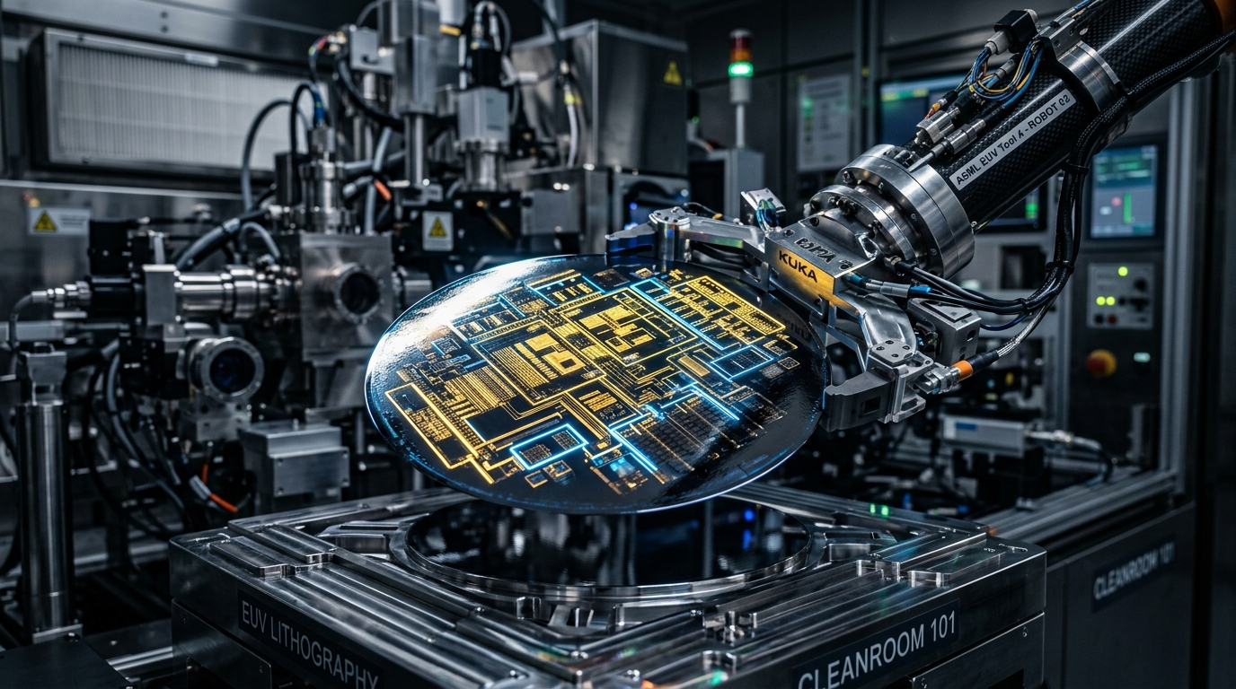
However, establishing leading-edge semiconductor foundries requires much more than cleanroom real estate. A viable wafer fab requires uninterrupted access to Ultra-Pure Water (UPW), extreme ultraviolet (EUV) photolithography scanners, high-purity chemical gases, and automated material handling systems that sustain advanced chip fabrication.
How the Semiconductor Industry Is Adapting to Custom Hyperscaler Silicon
In response to supply bottlenecks and high merchant silicon pricing, major cloud hyperscalers are actively designing proprietary Application-Specific Integrated Circuits (ASICs) tailored precisely to their internal software stacks, reshaping business models across the semiconductor market.
Recent disclosures from technology leaders like Alibaba detailing next-generation multi-trillion parameter models and proprietary AI accelerators (such as the Zhenwu V900 architecture) demonstrate that the sector is moving toward vertical full-stack integration. By co-designing compiler frameworks with bespoke silicon instruction sets, hyperscalers can achieve up to 3x energy efficiency improvements over off-the-shelf general-purpose processors.
For developers exploring modern software performance and API data architectures, explore our Developer Tools Hub and JSON Code Formatter to inspect complex network payloads.
Comparison Matrix: Modern AI Chip Architectures, Nodes, and Applications
The following technical reference matrix compares leading processing architectures within the global computing landscape across primary manufacturing nodes, interconnect technologies, power consumption, and enterprise deployment scenarios:
| Processing Architecture | Dominant Process Node | Memory Subsystem | Interconnect Technology | Power Envelope (TDP) | Primary Workload Optimization |
|---|---|---|---|---|---|
| Enterprise AI GPUs | 3nm – 2nm GAAFET | HBM3e / HBM4 (144GB+) | NVLink / PCIe Gen 6 | 700W – 1000W+ | LLM Pre-Training, Multimodal Generative AI |
| Custom Hyperscaler ASICs | 4nm – 3nm FinFET | Integrated HBM / LPDDR5 | Proprietary Optical Fabrics | 350W – 600W | Targeted Transformer Inference & Search |
| Edge Neural Processors (NPUs) | 5nm – 4nm | Unified On-Die SRAM | Direct Memory Bus | 5W – 25W | Smartphones, Wearables, Computer Vision |
| 2nm Optical Transceivers | 2nm Photonic Dies | Ultra-Low Latency Buffers | Co-Packaged Optics (CPO) | 15W – 40W | Inter-Cluster Terabit Switch Routing |
The Networking Bottleneck: High-Speed 2nm Optical Interconnects
As artificial intelligence clusters expand beyond 100,000 GPUs, standard copper cabling reaches its physical transmission and thermal limits. When thousands of processors must synchronize model weights across distributed nodes, network latency can throttle computing efficiency by up to 40%.
To overcome this communication barrier, innovators are deploying 2nm optical communication engines. Demonstrations by companies such as Marvell Technology highlight the rise of Co-Packaged Optics (CPO)—integrating photonic optical transceivers directly onto the processor substrate. This reduces electrical resistance, cuts networking latency to nanoseconds, and slashes interconnect power consumption by over 30% across modern data centers.
Photonic integrated circuits (PICs) represent the next grand milestone for high-speed computing. By replacing copper traces with microscopic silicon optical waveguides, signals travel literally at the speed of light with virtually zero parasitic capacitance.
The Semiconductor Industry Energy Paradox: Gigawatt Grids & Cooling
The rapid expansion of the semiconductor industry faces a formidable physical constraint: electrical grid capacity and thermodynamic dissipation.
- Gigawatt-Scale Data Centers: Next-generation AI campuses demand electrical power equivalent to entire mid-sized cities, accelerating investments in dedicated nuclear small modular reactors (SMRs) and renewable microgrids.
- Direct-to-Chip Liquid Cooling: With modern AI accelerators generating over 1,000 watts of heat per socket, traditional air conditioning has been replaced by closed-loop dielectric liquid cooling and two-phase immersion systems.
- Thermodynamic Silicon Optimization: Chip designers are adopting Gate-All-Around (GAA) nanosheet transistors and backside power delivery networks (BSPDN) to minimize parasitic capacitance and reduce power leakage at 2nm nodes.
Discover more about digital systems infrastructure in our guide to Data Center Efficiency Calculations and Physical Power & Storage Unit Conversions.
Future Outlook: What the Semiconductor Industry Evolution Means for Consumers
While cutting-edge 2nm silicon is initially deployed in industrial AI supercomputers, architectural innovations pioneered within the semiconductor industry rapidly trickle down into consumer electronics:
- Local In-Browser AI: Consumer laptops and workstations will run multi-billion parameter language models locally in device RAM with zero cloud latency.
- Intelligent Wearables: Ultra-low-power NPUs enable smart glasses and AI earbuds to perform computer vision and noise filtering on a single daily battery charge.
- Next-Gen Automotive Automation: Real-time neural inference chips provide instantaneous Level 3 and Level 4 autonomous driving safety checks.
Frequently Asked Questions About the Semiconductor Industry
Here are concise, authoritative answers to common questions regarding chip manufacturing, AI hardware, and global technology trends: